8x8x8 LED Cube
|
Creator: |
Contents
Overview
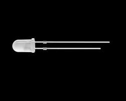
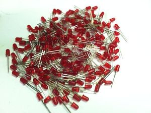
I purchased a bunch of LED's a few years ago with the intention of making LED Christmas lights with them. Here is what they look like:
I got lazy and decided I didn't want to do that project. In early May of 2012, I decided that I wanted to do something with those LED's. So I Googled LED projects and found this 8x8x8 LED Cube. I thought it was the coolest project ever so I decided I wanted to try it. Here is how I did it...
How The Cube Works
This is an 8x8x8 cube which has 512 LED's.
An LED has two legs. One leg is called the anode, which is the positive longer leg, and the cathode, which is the negative shorter leg.
The LED cube is made up of columns and layers. The cathode legs of every LED in a layer are soldered together. All the anode legs in one column are soldered together. There are 8 layers which have 64 LED's on each layer and there are 64 columns.
Each of the 64 columns are connected to the controller board with a separate wire. Each column can be controlled individually. Each of the 8 layers also have a separate wire going to the controller board.
Each of the layers are connected to a transistor that enables the cube to turn on and off the flow of current through each layer.
By only turning on the transistor for one layer, current from the anode columns can only flow through that layer. The transistors for the other layers are off, and the image outputted on the 64 anode wires are only shown on the selected layer.
To display the next layer, simply turn off the transistor for the current layer, change the image on the 64 anode wires to the image for the next layer. Then turn on the transistor for the next layer. Rinse and repeat very very fast.
NOTE: Taken from 8x8x8 LED Cube
First Cube
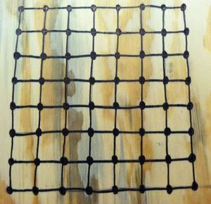
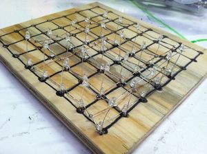
As stated in the previous section, the cathode legs of every LED are soldered together to form the layers of the cube. The easiest way to solder the LEDs together is to create a jig. Here is a pic of the first jig I created:
I knew I didn't want to use the LEDs I originally purchased for the Christmas lights because they are really flimsy. So I decided to use them to practice my soldering skills which would also allow me to figure out how the cube works. I started with a 5x5x5 cube.
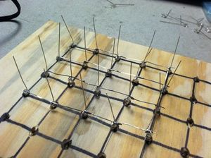
I started soldering the cathode legs together.
I then soldered a piece of wire across the cathode leg of the LEDs to add support.
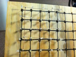
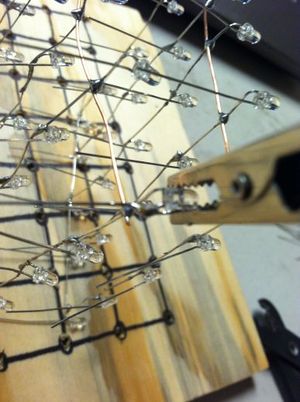
Once I got 1 layer done, I created another layer so I could figure out how to solder the anode layers together. I used an alligator clip to keep the LED leg where I wanted it.
Once I got the anode legs soldered together, I had a 5x5x2 LED Cube.
I stopped at this point because I had a pretty good understanding of how to create the cube.
Second Cube
At this point I ran out of the White LED's. Luckily, one of our members Scott bought out one of the electronic stores here in Huntsville...so he had some LED's to spare.
Creating The Jig
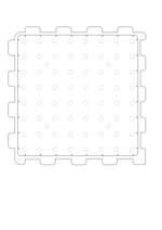
These LED's were much larger that the LED's I originally started out with. So now that I had larger LED's, I needed a jig that could support these larger LED's. So Scott created a new jig in Inkscape. This new jig ended up adding extra support to the cube. We used acrylic for the new cube and used the Laser Cutter to create the jig. Below is the .svg file we used to create the jig. You can right click on the .svg file to save it and create a jig for yourself if you would like to attempt this project.
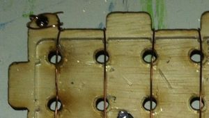
This jig requires two separate pieces. The "Bottom" piece in the .svg file should be cut out of a thick piece of acrylic because wire will be wrapped around this piece. The "Top" piece can be cut out of a small piece of acrylic.
I wanted to test the jig to make sure everything lined up properly. So the bottom was cut out of a think piece of wood and the top was cut out of a piece of acrylic.
The top piece is placed on top of the bottom piece making sure the holes line up. Screws and nuts were then placed in the 4 holes that are around the middle of the jig.
Wrapping Wire Around The Jig
Like I said in the previous section, this jig adds extra support to the cube because of the criss cross like way the wire is wrapped around the jig.
To start wrapping the jig, place the end of a long piece of wire around the top left hole of the bottom piece of the jig. Around the wire around tab a couple of times.
Etching the Driver Board
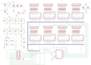
In order to control the cube, it has a driver board and a controller or power board. I started putting together the driver board first because I had all the parts I needed. I started putting the board together based off of this schematic:
I soldered the IC socket's for the 74HC574N IC's and the 74ACT138N IC on a prototype pcb board. I started making the connections for pins 1-11 of the 74HC574N IC. I thought I was supposed to solder pins 1-11 of each IC together and then solder those pins into something else. I didn't know what that something else was but I was going to figure it out later. I quickly learned I was wrong.
A bus works by connecting one pin of all 8 of the 74HC574N IC's together. So pin 1 of all the 74HC574N IC's are soldered together. All of pin number 2 of the 8 IC's are soldered together. And so on and so forth.
I asked Scott if I was wiring the board up correctly and I was quickly shot down. Scott explained to me what a bus was. I learned that it would have taking a lot of wire to accomplish creating a bus with 8 IC's. So Scott suggested we etch the driver board. This turned into a 3 day ordeal.
Here's the process of etching the board:
The first thing we had to do was look a the schematic for the driver board from the instructables site. Scott quickly realized that the schematic was created from eagle, an application to create pcb's. We copied the schematic off of the instructables site and imported it into eagle. We were limited to a space of 4" by 3". So we had to rearrange the IC's and resistors to fit in this space. In about 6 hours of editing, we had a board ready to be printed and etched. This board would have a top layer and a bottom layer.
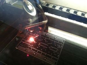
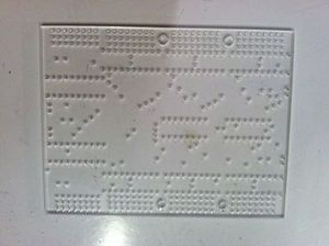
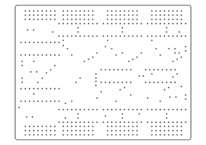
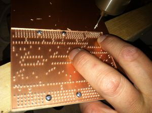
But before we could print the board, we needed to create the holes for the components. The laser cutter can't cut copper clad boards. So we came up with the next great idea. We imported just the holes of the board into Inkscape and created a jig for drilling holes in the copper clad board.
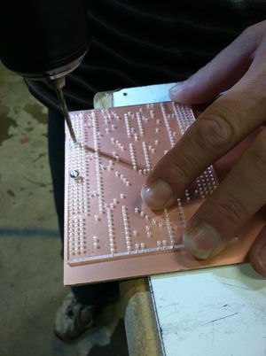
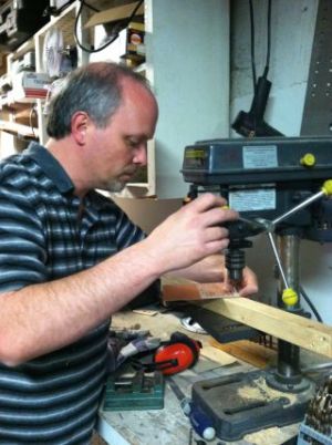
Now that we had to jig for putting the holes in the copper clad board, we had to drill the holes.
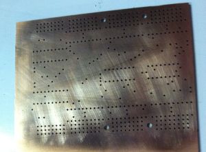
[File:Finished drilling holes.jpg|thumb|none|300px|Holes drilled out]]
Next we had to get rid of any oil on the copper clad board. If oil was left on the board, the transfer paper wouldn't stick to the board and we would have to redo the whole process over again. So we took steel wool and scrapped the copper clad board to get rid of any oils.
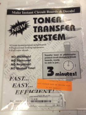
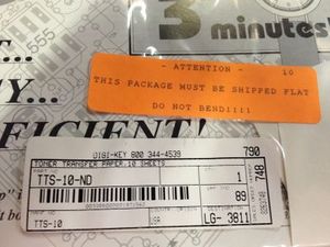
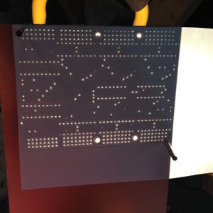
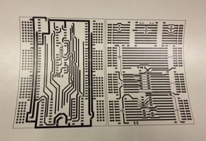
Now we were ready to place the circuit on the board. We exported our schematic to a .bmp file so we could save it to a .doc file to be printed. We had to make a negative of the top layer in order for it to be etched properly. We used Toner Transfer paper from Digi-Key. We got the document printed at Staples for less than 30 cents. The document had to be printed on a laser printer on the shiny side of the transfer paper otherwise the transfer wouldn't work.
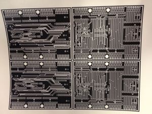
The board with the horizontal traces is the top layer and the one with the vertical traces is the bottom layer. We cut out the top layer and bottom layer that we needed. We then lined the holes of the transfer paper up with the holes of the copper clad board.
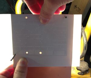
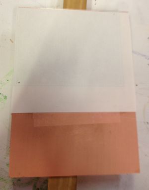
We then placed tape on the transfer paper and the copper clad board to keep the transfer paper from skewing off when it goes through the laminator. We later learned that the tape would melt off and get all over the inside of the laminator. But more on that later.
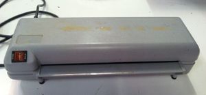
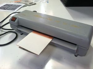
Now we were ready to laminate the transfer paper onto the copper clad board.
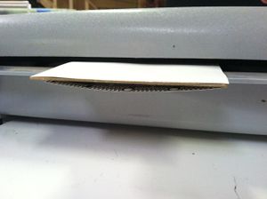
Laminating Transfer Paper to Copper Clad Board Front End
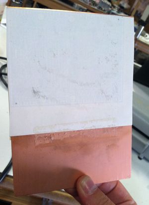
Finishing Laminating Copper Clad Board
Next, we had to place the laminated copper clad board in water to get the transfer paper off of the copper clad board. The transfer paper is water soluble. So when the board is placed in water, the transfer paper will come off leaving the toner with the circuit on the copper clad board. In the video below, Scott see's that a finger print appears on one of the traces. I assume that the finger print was left on the copper clad board when we were placing the transfer paper on the copper clad board. Scott thought that the finger print was left on the transfer paper. We later learned that Scott was wrong and Jennifer was right! :) The finger print was indeed left on the copper clad board. We didn't scrap the copper clad board with steel wool to get rid of any excess oil before placing the transfer paper on the copper clad board...FAIL!! :(
Copper Clad Board Being Placed in Water
Finger Print on the Copper Clad Board
So now that the circuit had a finger print on it, the board had to be redone. So we took steel wool to the copper clad board and started over again :(
We thought that this was going to be an easy process. Boy were we wrong. It took us 5 more times to get a board that we were satisfied with. Here is what we learned and the problems we had:
1.) A finger print was left on copper clad board...see the video above
2.) Before we put the copper clad board through the laminator, we had to tape the transfer paper to the copper clad board. In this second iteration, the laminator melted the tape leaving parts of the laminator with gummy crap on it. This gummy crap was in the middle of the laminator. We decided to not clean it out for the third iteration.
3.) Because the laminator had gummy crap on it, we had to place the copper clad board near the end of the laminator. The laminator decided to eat the copper clad board. Thus, forcing us to take the laminator apart to clean it.
4.) Now we had a clean laminator! :) But we used all of our transfer paper with the circuit printed on it. Staples was closed. So we had to go to the next best thing...Kinko's...which was open 24 hours. We ended up re-doing the circuit to minimize on the amount of traces. There was a problem with Kinko's toner. It sucks!! The traces came off during the soaking in water process. Forcing us to do it for a 5th time.
5.)
Hack A Day
One day, Caleb Kraft, from Hack A Day decided to visit the shop. I happened to be working on my cube when he came. So he asked me a few questions about the cube. Here is the link:
YAY!!
