Here are some basic instructions for creating a solder stencil from an EagleCad board layout. The instructions should be relatively portable from application to application; if your layout software can provide a gerber file with the appropriate holes in it, it should be possible to make a stencil from it. The stencil will be used to apply solder paste to the board, and then a skillet will be used to solder all of the components at the same time.

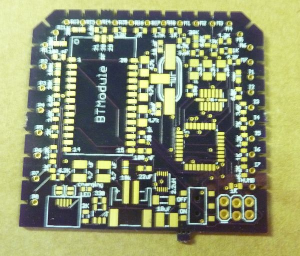
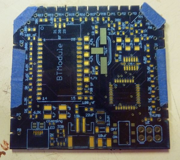
Let's say you have this SMD board that needs populating and you are too scared/lazy to populate the whole thing by hand.

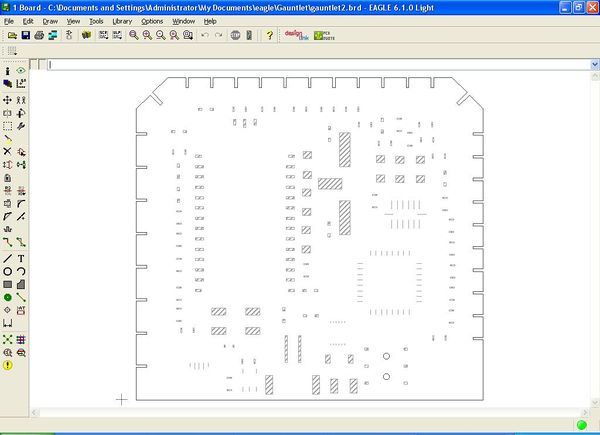
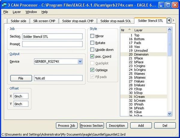
Assuming you have the original cad files, it should be possible to generate a stencil on the laser cutter. Eagle holds the pertinent information on the Dimension (board outline) and tCream (solder stencil) layers.

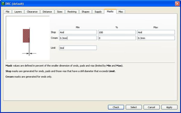
In order to control the size of the aperatures for the solder stencil, you need to go into the DRC tool and change the size parameter (maybe it makes sense to have configuration options in the 'design rule check' tool if you read the directions in German?). I decided on .3mm through an iterative guess-and-check process. This value will depend on the size of your pads and thickness of your stencil.

Once you're happy with the aperature size, you can create a new export layer for the default gerber CAM job. Any CAM job can be modified; simply clicked 'Add', gave it a file name, and selected the appropriate layers. Running this CAM job creates a *.stl file with the cuts specified.

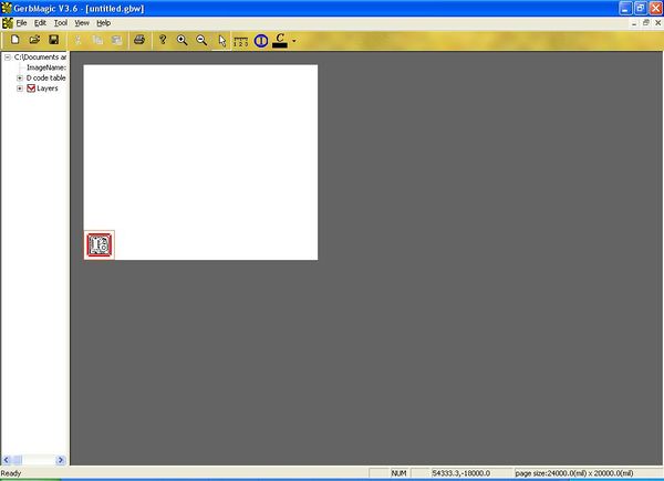
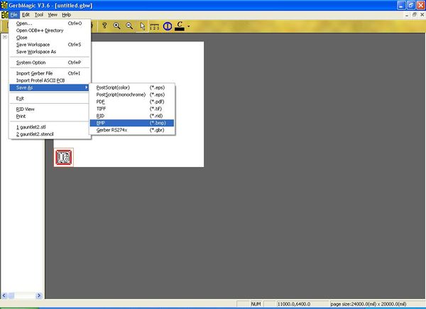
In order to extract the information from the gerber file, I need to get it into a format that inkspace understands. To do this I used GerbMagic to import the file and then export it in bitmap format.

Export to BMP, God's own format.

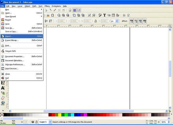
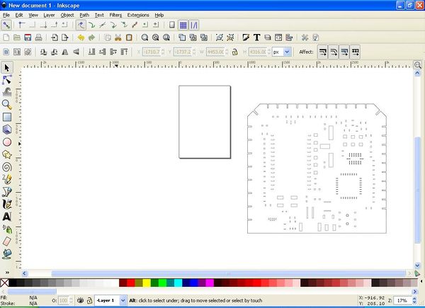
Now the solder stencil information is in bitmap form, and can be loaded into Inkscape using 'Import'.

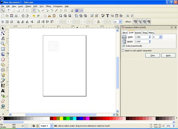
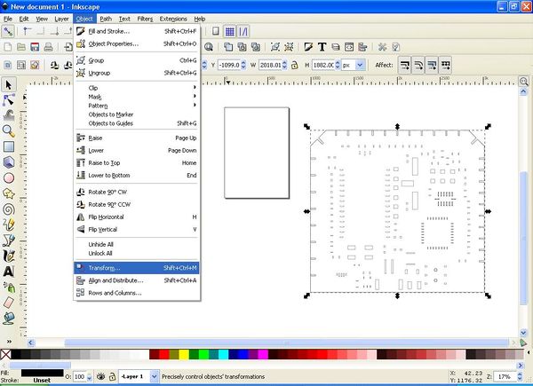
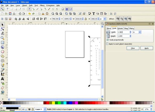
Unfortunately the conversion to bitmap hosed all of the dimensional information. Eaglecad can be used to read the actual size of the board and we can use this resize the imported bitmap.

I had the most luck letting Inkscape maintain the ratio and just putting in the most convenient dimension; in this case, width.

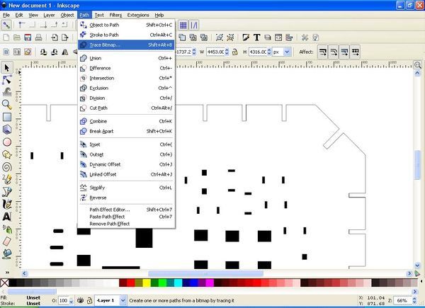
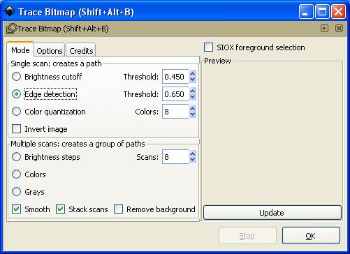
Once the drawing is the right size to match the physical board, you can trace the image to form vectors.

I used edge detection because of the high-contrast bw source image and the fact the edges are what I care about, but there may be a better way.

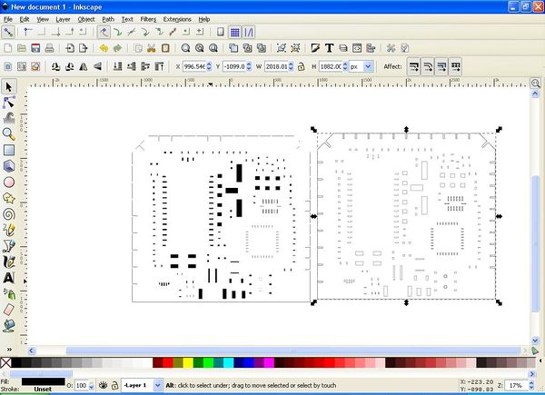
Now that the trace is done, seperate the two boards (vector object and raster object) and delete the raster object. The raster object will be the one with the solid spaces.

Once you have a the scaled vector image, you are ready to print to the laser cutter. I printed to both cardstock and stencil plastic (both with the typical cardstock settings to cut through) and was happy with both. In the long run I think a plastic stencil would last longer (and can be washed to be reused at a later date), but if longevity is truely a concern, nothing beats a metal stencil.

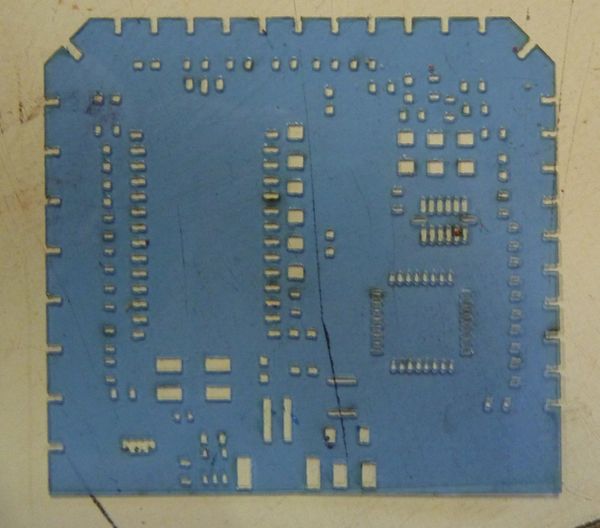
Now we have the cut out stencil.

Attach it to the board, making sure it is flat against the surface and lined up accurately.

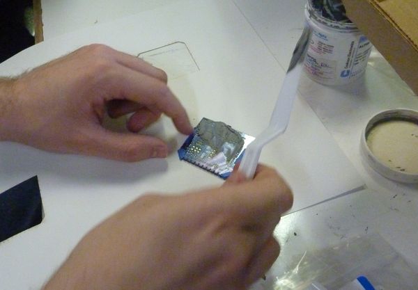
Spread solder paste across the whole board, making sure to get an even amount of solder into all of the voids.

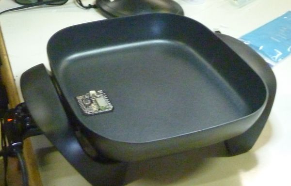
After spreading the solder paste, remove the mask and carefully place components. Once the board has been populated, place it on the skillet.

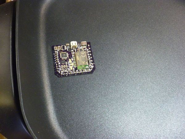
Cook at 400F until the paste phase changes, then turn off the heat and remove the board once the solder hardens.
